Revolutionary Solutions for Manufacturing Test Required
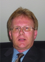
Peter Muhmentaler, Director Test Solution Infineon Technologies AG
Abstract
This talk refers to the economic constraints as they occur in manufacturing of microelectronic systems. Especially the situation for the mandatory manufacturing test will be explained. This leads to the structure of the test flow as it follows the essential steps of creating integrated circuits. Examples from wire line and wireless communication chips are taken to illustrate the semiconductor industry’s current state of the art in testing. The overall test cost of a microelectronic system is structured into the effort for test development as well as the product characterization and operation of volume testing. Both test applications are affected by so called test partitioning which will be described in more detail. Most recent developments in test equipment industry which require more and more EDA support and preferably encapsulation into the design flow will be commented. Even more emphasis is put on EDA contribution if it comes to revolutionary new Design for Test (DfT) approaches targeting the chip level as well as the intermediate hardware between test equipment and the device under test. The so called load board is a challenging key object in cost effective test solutions which may drive given EDA tools and development methodology to its limits. Hot topics in the current ITRS update process and their interaction with other disciplines like package technology will be explained. New EDA solutions have to enable seamless product development and manufacturing flows which manifest in automatic diagnosis of test results. An outline of such leading edge tool flow will conclude the talk.
Curriculum Vitae
 Peter Muhmenthaler received a Diploma in electrical engineering from the University of Hannover, Germany, in 1988. Since 1989 he is with Infineon Technologies, the former Siemens Semiconductors. Starting with test engineering for DRAMs he moved to design flow development in 1991 with a special focus on macro cell and IP development. In 1995 he built up the center of competence for VLSI test methodology and design for testability. Since 2002 he is director test solutions in the corporate test technology organization.


